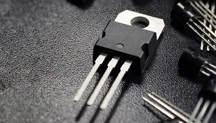
A transistor is a semiconductor device with at least three terminals that can not only amplify electrical signals but also function as a switch. Transistors are roughly divided into bipolar transistors (BJTs) and field-effect transistors (FETs), depending on their structure. In addition, there are insulated gate bipolar transistors (IGBTs) with MOSFET characteristics in the input stage and BJT characteristics in the output stage.
Transistors are used in various electronic devices, mainly for switching (on/off) or amplifying electrical signals in circuits. Examples of switches include circuits that turn on/off at logic signal levels (up to 5V) and switch power supplies. Amplification circuits are not only used for simple signal amplification, but also for oscillation circuits.
Types and characteristics of transistors
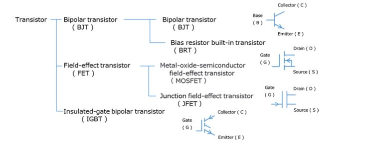
Types and symbols of transistors
Bipolar Transistor(BJT)
BJTs have two pn junctions that use electrons and holes as charge carriers, hence they are called bipolar transistors. BJT has three terminals: base, collector, and emitter. This type of transistor is divided into two categories: NPN-BJT and PNP-BJT.
The collector current flows in proportion to the current flowing from the base to the emitter (base current). Therefore, BJT is called a current control element. When the base current does not flow, the transistor is in an off state.
Usually, voltage is used as the control signal for BJTs, and the control voltage is converted into current through a resistor and input to the base.
Bias resistor built-in transistor (BRT) is a bipolar transistor with built-in resistor, mainly used as a switch.
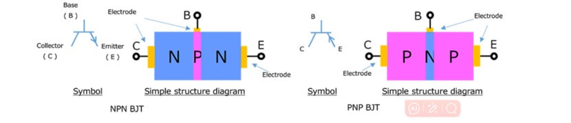
BJT notation and simplified structure
Unlike MOSFETs, BJTs require current to be transmitted to the base, so the device consumes more energy than MOSFETs. Although the switching speed is slow, it is easy to make it resistant to high voltage. In addition, it also has the characteristics of easy gain and high amplification factor. BJTs are used in circuits that require high amplification factors. Due to the conductivity modulation effect (minority carrier accumulation effect), BJTs have a lower voltage drop at saturation, but this effect also has a disadvantage of prolonging the transition time from conduction to turn off.
Field-effect transistor (FET)
FET is a transistor that does not have a pn junction on the path through which current flows, and only uses electrons or holes as charge carriers. Therefore, it is also known as a unipolar transistor, in contrast to bipolar transistors. FET can be divided into two categories: one is metal oxide semiconductor field-effect transistor (MOSFET) mainly used for switching, and the other is junction field-effect transistor (JFET) mainly used for amplifiers.
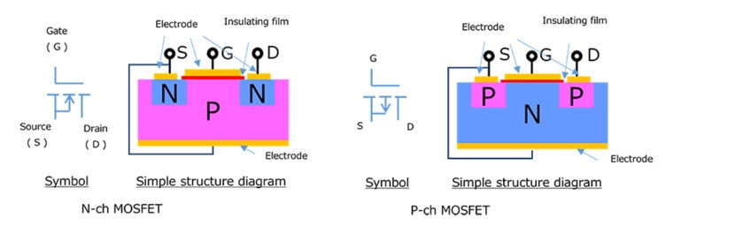
Symbol and Simplified Structure of MOSFET
FET has three terminals: gate, drain, and source.
The voltage applied between the gate and source (gate voltage) can achieve the conduction and turn off of the component. In the saturation region, the magnitude of the output current varies correspondingly with the magnitude of the gate voltage. Therefore, FET is called a voltage control element.
The gate terminal is insulated from other terminals, so no current flows except for charging the parasitic capacitance. Its characteristics include low driving current and high-speed switching
Insulated gate bipolar transistor(IGBT)
IGBT is a device that combines the characteristics of MOSFET and BJT. It is a product that combines the high-speed switching characteristics of MOSFETs with the low conduction voltage (low saturation drop) characteristics of BJTs. IGBT uses electrons and holes as charge carriers during operation, so it is sometimes classified as a bipolar transistor.
IGBT has three terminals: gate, collector, and emitter
What is the composition of a transistor?
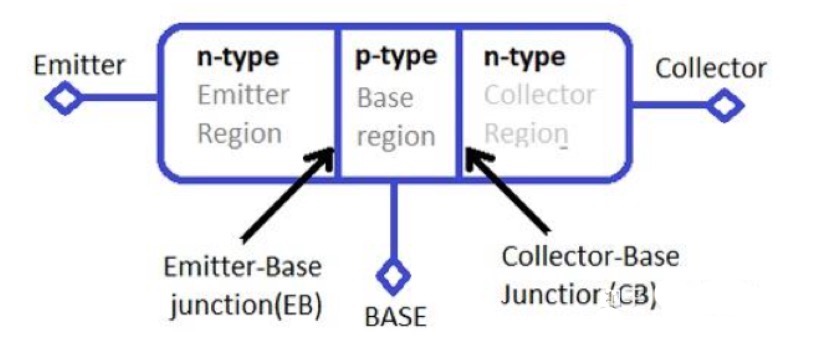
Transistors are composed of three layers of semiconductors, which have the ability to maintain current. Conductive materials such as silicon and germanium have the ability to transmit current between conductors and insulators surrounded by plastic wires. Semiconductor materials are processed through a chemical process called semiconductor doping. If arsenic, phosphorus, and antimony are doped into silicon, it will acquire some additional charge carriers, namely electrons, known as N-type or negative semiconductors; If silicon is doped with other impurities such as boron, gallium, or aluminum, it will obtain fewer charge carriers, i.e. holes, known as P-type or positive semiconductors.
How do transistors work?
We will take NPN transistors as an example to illustrate the working principle of transistors. To understand how these components function as switches, the method is simple: imagine water flowing through a valve controlled pipe. Water pressure represents’ voltage ‘, and the flow of water through the water pipe represents’ current’ (Figure 3). The large water pipe represents the collector/emitter junction, separated by valves in the middle. The valves in the figure are represented by gray ellipses, like a movable baffle, and are activated by the water flow in the small water pipe representing the base. The valve maintains water pressure from the collector to the emitter. When water flows through a smaller water pipe (base), the valve between the collector/emitter junction will be opened, allowing the water to flow through the emitter to the ground (ground represents all water or voltage/current circuits).
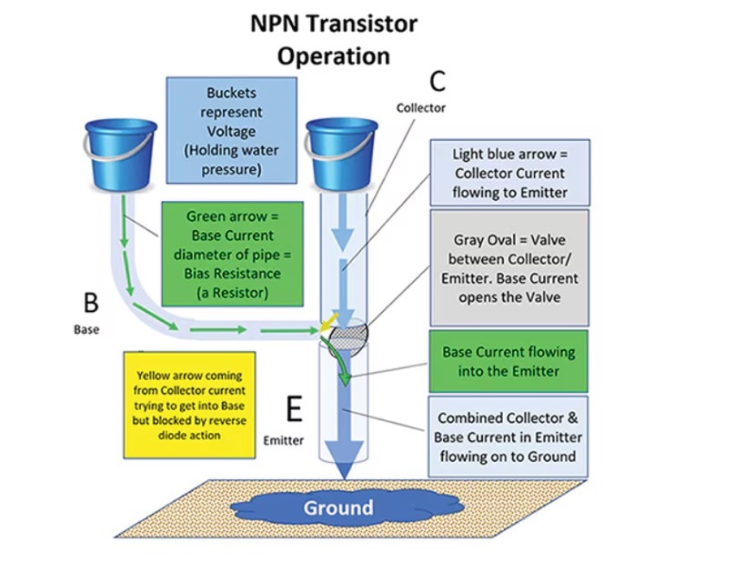
This figure illustrates the working principle of transistors in a graphical manner. When the water flows through the small water pipe (base), the valve between the collector/emitter junction will be opened, allowing the water to flow through the emitter to the ground
Select transistor based on application
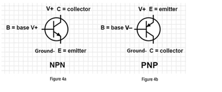
If you only want to turn on the circuit or load, you should consider the following points. Determine whether you want to bias or excite transistor switches with positive or negative current (i.e. NPN or PNP type, respectively). NPN transistors are driven (or turned on) by a positive current biased at the base to control the current from the collector to the emitter. PNP transistors are driven by a negative current biased at the base to control the current from the emitter to the collector. (Note that PNP polarity is opposite to NPN.) For more detailed information, please refer to the following figure.

There are several different kinds of transistors at Topdiode, NPN PNP THT & SMD TYPE
Topdiode produces PIN to PIN alternative to replace TVS DIODE from Littelfuse, Infineon, Vishay, Nexperia etc.
Cost down 30~60%,
Better lead time
Engineer team to do “cross to”
Support sample in free & trial order
Simply send RFQ to lily@topdiode.com for quote of transistors .
There will be experienced engineers do cross reference and choose the match series for you.