What is Transistor?
A transistor is a semiconductor device that can be used for amplification, switching, and signal modulation. It is a fundamental building block of electronic circuits and is widely used in various electronic devices. Transistors come in different types, such as bipolar junction transistors (BJTs) and field-effect transistors (FETs), each with its own variations.
Types of Transistors
There are two main types of transistors: Bipolar Junction Transistors (BJTs) and Field-Effect Transistors (FETs). Each type has different variations that serve specific purposes in electronic circuits. Here’s an overview of these two main types and their subtypes:
1.Bipolar Junction Transistors (BJTs):
a.NPN Transistor:
– Structure: Consists of three semiconductor layers—n-type (negative), p-type (positive),and n-type.
– Operation: Current flows from the collector (C) to the emitter (E) when a small current is applied to the base (B).
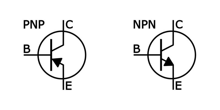
b.PNP Transistor:
– Structure: Similar to NPN but with the opposite arrangement of semiconductor layers—p-type, n-type, and p-type.
– Operation: Current flows from the emitter (E) to the collector (C) when a small current is applied to the base (B).
c.Darlington Transistor:
– Structure: Two transistors connected in series, often NPN-NPN or PNP-PNP.
– Operation: Provides higher current gain than a single transistor.
d.Heterojunction Bipolar Transistor (HBT):
– Structure: Combines materials with different bandgaps in the transistor’s layers.
– Advantages: Improved performance at high frequencies and lower power consumption.
- Field-Effect Transistors (FETs):
a.Junction Field-Effect Transistor (JFET):
– Types: N-channel JFET and P-channel JFET.
– Operation: Voltage applied to the gate controls the current flow between the source and drain.
b.Metal-Oxide-Semiconductor FET (MOSFET):
– Types:
– N-Channel MOSFET: Electrons carry the current.
– P-Channel MOSFET: Holes carry the current.
– Structure: Insulating oxide layer between the metal gate and semiconductor material.
– Operation: Voltage applied to the gate controls the flow of current between the source and drain.
c.Insulated Gate Bipolar Transistor (IGBT):
– Structure: Combines characteristics of MOSFET and BJT.
– Operation: Voltage control at the gate, current-carrying capability of a BJT.
d.Metal-Semiconductor FET (MESFET):
– Structure: Typically used in compound semiconductors like gallium arsenide (GaAs).
– Operation: Similar to MOSFET but with a metal-semiconductor junction.
These transistor types have various applications in electronic circuits, such as amplification, switching, and signal processing. The choice between BJT and FET often depends on the specific requirements of a given application, including factors like voltage levels, current requirements, and frequency of operation.
What is Small Signal Transistor?
Small Signal Transistors are a category of transistors designed and optimized for amplifying small electronic signals. They are primarily used in applications where the amplification of weak signals is required without affecting the overall characteristics of the signal. These transistors are often employed in analog circuits for amplification purposes.
How Small Signal Transistors works?
A transistor is essentially a switch that can control the flow of electric current. It has three terminals: the emitter, the base, and the collector in a Bipolar Junction Transistor (BJT), or the source, the gate, and the drain in a Field-Effect Transistor (FET). The behavior of the transistor depends on the voltages applied to these terminals.
In a BJT, a small current applied to the base-emitter junction allows a much larger current to flow from the emitter to the collector. This current amplification is a key feature of BJTs. The ratio of the output current (collector current) to the input current (base current) is called the current gain, denoted by the symbol β.
In a FET, the flow of charge carriers between the source and drain terminals is controlled by an electric field, which is created by applying a voltage to the gate terminal. Unlike BJTs, FETs do not require a base current to operate, which makes them more energy-efficient.
The ability of transistors to control the flow of electric current makes them useful in a wide range of applications. They can be used to amplify signals, as in audio amplifiers and radio transmitters, or to switch signals on and off, as in digital circuits. By combining millions or even billions of transistors on a single chip, it is possible to create complex electronic devices like microprocessors and memory chips.
What is the Keep Characteristics of Small Signal Transistors?
The key characteristics of small signal transistors include:
- Low Power Handling: Small signal transistors are designed to handle relatively low power levels compared to power transistors. They are typically used in applications where the power levels are in the milliwatt range.
- High Voltage Gain: Small signal transistors are optimized for high voltage gain, making them suitable for amplifying weak signals without introducing significant distortion.
- Low Noise: In applications where signal fidelity is crucial, such as in audio amplifiers or communication systems, small signal transistors are designed to minimize electronic noise, ensuring a clean output signal.
- High Input Impedance: Small signal transistors usually have a high input impedance, which means they draw minimal current from the source they are amplifying. This is advantageous when interfacing with circuits that have high output impedance.
- Small Physical Size: Small signal transistors are often physically smaller than power transistors, making them suitable for integration into compact electronic circuits.
- Common types of small signal transistors include Bipolar Junction Transistors (BJTs), such as NPN (Negative-Positive-Negative) and PNP (Positive-Negative-Positive) transistors, as well as Field-Effect Transistors (FETs).
What is Materials and Manufacturing Process of Transistor?
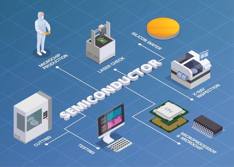
Transistors are semiconductor devices, and their construction involves specific materials and manufacturing processes. The two main types of transistors, Bipolar Junction Transistors (BJTs) and Field-Effect Transistors (FETs), have slightly different structures, but both are based on semiconductor materials. Silicon is the most widely used semiconductor material in transistor manufacturing due to its favorable properties. Here’s an overview of the materials and manufacturing processes involved:
Materials:
- Semiconductor Material:
- BJTs: Typically made of silicon (Si), though germanium (Ge) was used in earlier devices.
- FETs: Primarily made of silicon, but other semiconductor materials like gallium arsenide (GaAs) or silicon carbide (SiC) may be used for specialized applications.
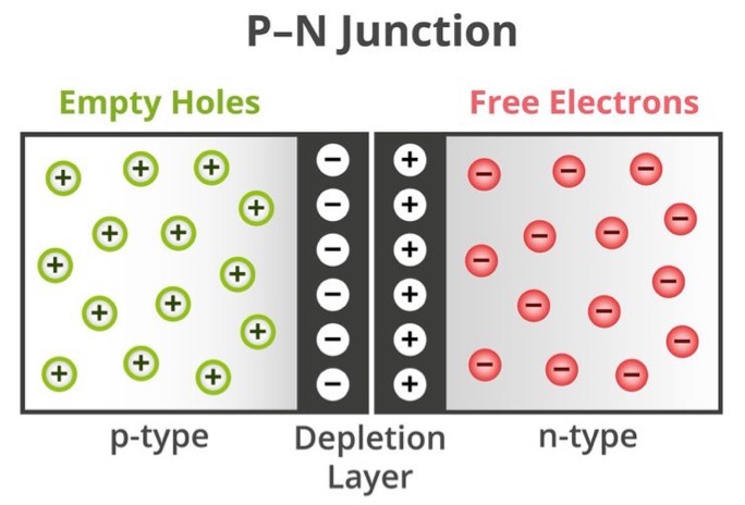
- Doping Agents:
- Semiconductors are doped with specific impurities to create regions with excess electrons (n-type) or holes (p-type).
- Common dopants include phosphorus (P) or arsenic (As) for n-type doping and boron (B) for p-type doping.
- Insulating Materials:
Oxides, such as silicon dioxide (SiO2), are used for insulation in certain areas of the transistor.
- Metal Contacts:
Metals like aluminum or copper are used to form electrical contacts.
Manufacturing Process (for Silicon-based transistors):

- Crystal Growth:
Silicon crystals are grown using the Czochralski process or other methods.
- Wafer Formation:
The silicon crystal is sliced into thin wafers using a diamond saw.
- Doping:
The wafer is treated with dopant materials through processes like diffusion or ion implantation to create n-type and p-type regions.
- Oxidation:
A thin layer of silicon dioxide is grown on the wafer’s surface to serve as an insulator.
- Photolithography:
A photoresist is applied, exposed to UV light through a mask, and developed to create a pattern on the wafer.
- Etching:
Unwanted material is selectively removed using etching chemicals, leaving the desired pattern.
- Deposition:
Thin layers of materials (metals, insulators) are deposited on the wafer’s surface using techniques like chemical vapor deposition (CVD).\
- Metallization:
Metal contacts are formed by depositing and patterning metal layers.
- Testing and Packaging:
Each transistor is tested for functionality and performance. Transistors are then packaged to protect them and provide electrical connections.
The exact manufacturing processes can vary based on the type of transistor, technology node, and specific application requirements. Advanced techniques, such as photolithography and thin-film deposition, play crucial roles in creating the intricate patterns and structures on the semiconductor wafer. The evolution of transistor technology has led to smaller sizes, increased integration, and improved performance over the years.
Topdiode Small Signal Transistors Introduction
Topdiode is manufacturer for small signal transistors in China. Topdiode offer fast delivery for small signal transistors. Topdiode is very competitive supplier for small signal transistors BC807 BC808 PNP Silicon Epitaxial Planar Transistors, BC856 BC857 BC858 BC859 BC860 Small Signal Transistor, MMBT3906 PNP Silicon General Purpose Transistor, BC817 BC818 NPN Silicon Epitaxial Transistor, MMBTA14 NPN Silicon Epitaxial Planar Transistors, BC846DW~BC850DW, MMBT7002, 2N2907-2N2907A, MMBT458, TLT6354SL, BC8456DE-BC8458DB, MPSA42U, BC856W~BC860W.
Topdiode Small Signal Transistors Key features and Benefits
Broad choice of SMD and leaded package options
SOT-89, SOT-23/SOT-236, SOT-323, SOT-363, SOT563
Low voltage and high-voltage types available
Cost efficient replacement of NXP
Topdiode Small Signal Transistors Key applications
General purpose switching and amplification
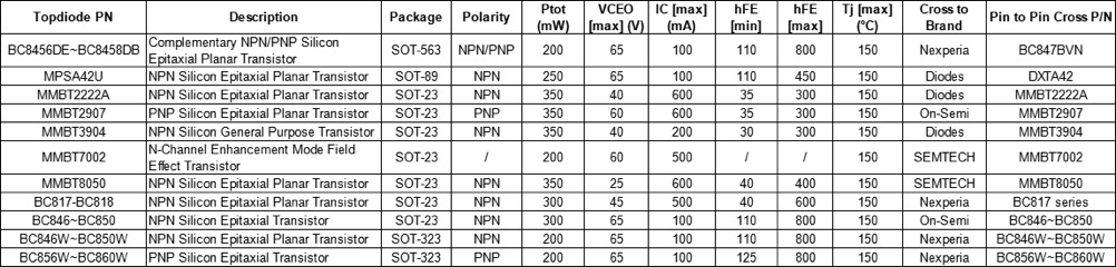
Topdiode Small Signal Transistors Parametric Table