NPN and PNP are two types of transistors. Transistors are semiconductor devices made of doped p-type and n-type junctions.
Transistors – NPN & PNP – Basic Introduction
Differences
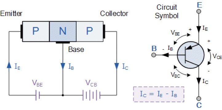
The transistor is consisted of a three-part semiconductor forming two PN junctions, and its composition forms are PNP type and NPN type. Most of the germanium transistors are of PNP type, and most of the silicon transistors are of NPN type. Their structural principles are the same. The triode has three regions and three electrodes. Among them, the base region (a thin layer of semiconductor in the middle of the triode) leads to the base b; there are emitter regions leading to the emitter e and collector regions leading to the collector c on both sides. The PN junction between the transmitting area and the base area is called the transmitting junction, and the PN junction between the collecting area and the base area is called the collecting junction. On the circuit symbol, the PNP tube emitter arrow points inward, and the NPN tube emitter arrow points outward, indicating the current direction.
NPN and PNP transistors are mainly different because the direction of current is different from the positive and negative of voltage. To be professional, it is the “polarity” issue. NPN uses the B-E current (IB) to control the C-E current (IC), the E pole has the lowest potential, and usually, the C pole has the highest potential during normal amplification, namely VC>VB>VE. PNP uses the E-B current (IB) to control the E-C current (IC). The E pole has the highest potential, and usually, the C pole has the lowest potential during normal amplification, that is, VC<VB<VE.
Difference in definitions
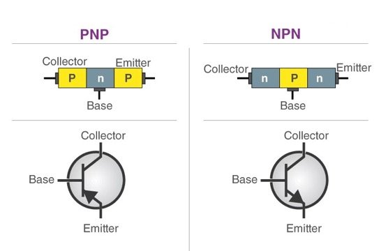
NPN transistor: It is consisted of two N-type semiconductors and one P-type semiconductor, with the P-type semiconductor in the middle and two N-type semiconductors on both sides. The triode is the most important device in electronic circuits, and its main function is the amplification and switching of current.
PNP transistor: A triode composed of two P-type semiconductors sandwiched between an N-type semiconductor, so it is called the PNP type triode. It can also be described as a transistor in which current flows from the emitter E.
Difference in circuit controlling
NPN: Use the current (IB) of B→E to control the current (IC) of C. The E pole has the lowest potential, and the C pole has the highest potential during normal amplification, that is, VC> VB> VE
PNP: Use E&B current (IB) to control E&C current (IC). The E pole has the highest potential, and the C pole has the lowest potential during normal amplification, that is, VC <VB <VE.
Other differences
The Output states of PNP and NPN sensors are different. They actually use the saturation and cut-off of the transistor to output two states, which are switch-type sensors. But the output signal is completely opposite, namely high level and low level. NPN output is low level 0, PNP output is a high level 1.
NPN transistors and PNP transistors are different in structure: NPN transistors consist of a p-type semiconductor sandwiched between two n-type semiconductors, while PNP transistors consist of n-type semiconductors sandwiched between two p-type semiconductors.
The majority of the carriers in NPN transistors are electrons, while most carriers in PNP transistors are electron holes.
When being used as switches, NPN transistors are faster to switch. When the triode is being used as a switch, it works in two states: cut-off and saturation. Generally, the conduction and disconnection of the transistor are controlled by controlling the base voltage Ub of the transistor.
Methods of distinguishing NPN transistors and PNP transistors
Identifying Base B
Set the digital multimeter to the diode position, connect the red test lead to a certain pin, and use the black test lead to touch the other two pins in turn. If the two displayed values are both less than 1V or the overflow symbol “1” is displayed, The connected pin that connects to the red test lead is base B. If in the two tests, one display value is less than 1V, another displays overflow symbol “1”, it indicates that the pin connected to the red test lead is not base B. Then you should change to other pins and measure them again until base B is found.
Then, use the diode file of the digital multimeter. After identifying base B according to the above operation, connect the red test lead to base B, and touch the other two pins with the black test lead. If both display 0.500~0.800V, the tested tube is of NPN type; if the overflow symbol “1” is displayed both times, it means that the tested tube is of PNP type.
Identifying Base
Use a multimeter R×100 or R×1k to measure the forward and reverse resistance values between every two of the three electrodes of the tube. When the first test lead is connected to a certain electrode, and the second test lead successively touches the other two electrodes and the low resistance values are measured, the electrode connected to the first test lead is base b. At this time, pay attention to the polarity of the test lead of the multimeter. If the red test lead is connected to base b, and the measured resistance of the black test lead connected to the other two poles is small, then the tested tube can be determined to be a PNP transistor; If the black test lead is connected to the base electrode b and the red test lead is connected to the other two electrodes, and the measured value of resistance is small, then the tested transistor is an NPN transistor.
Comparison of n-p-n Transistors and p-n-p Transistors which is better
n-p-n Transistors Most Preferred Over p-n-p Transistors
- Carrier Mobility – The majority charge carriers in n-p-n transistors are electrons unlike in p-n-p transistors where the majority charge carriers are holes. Electrons move far more easily than holes within the crystal lattice. As a result, they have higher mobility and operate faster providing a much better level of performance.
- Production Costs – The manufacture of silicon-based transistors is most economically carried out using large N-type silicon wafers. The manufacture of PNP transistors requires three times more surface area of the wafer, and this significantly increases the costs.
- Negative Grounding – Over the years, a negative ground has become standard and the polarity of NPN transistors means that the basic transistor configurations operate with a negative ground.
Application
There are PNP and NPN type of sensors(switch type), and they are divided into six categories:
- NPN-NO (normally open type)
- NPN-NC (normally closed type)
- NPN-NC+NO (common type of normally open and normally closed)
- PNP-NO (normally open type)
- PNP-NC (normally closed type)
- PNP-NC+NO (common type of normally open and normally closed)
PNP and NPN sensors generally have three lead wires, namely the power line VCC, the 0V line, and the OUT signal output line.
PNP type
When a signal is triggered, the signal output line OUT is connected to the power line VCC, and the PNP type of sensors is equivalent to a power line that outputs a high level.
For the PNP-NO type, when the signal is not triggered, the output line is suspended, that is, the VCC power line and the OUT line are disconnected. When the signal is triggered, the same voltage as the VCC power line is issued, that is, the OUT line is connected to the power line VCC, and a high-level VCC is output.
For the PNP-NC type, when the signal is not triggered, the same voltage as the VCC power line is sent, that is, the OUT line is connected to the power line VCC, and the high level VCC is output. When the signal is triggered, the output line is suspended, that is, the VCC power line is disconnected from the OUT line.
For the PNP-NC+NO type, there is actually an extra output line OUT, which can be selected according to needs.
NPN type
When a signal is triggered, the signal output line OUT is connected to the 0v line, and the PNP type of sensors are equivalent to outputting a low level of 0V.
For the NPN-NO type, when the signal is not triggered, the output line is floating, that is, the 0v line and the OUT line are disconnected. When the signal is triggered, the same voltage as 0V is issued, that is, the OUT line is connected to the 0V line, and the output is low level OV.
For the NPN-NC type, when the signal is not triggered, the same voltage as the 0V line is sent, that is, the OUT line is connected to the 0V line, and the low level 0V is output. When the signal is triggered, the output line is suspended, that is, the 0V line is disconnected from the OUT line.
The PNP-NC+NO type is similar to the NPN-NC+NO type. There is one more output line OUT, and two output lines with inverted signals. They need to be chosen according to needs.
FAQs
Q1: What does the arrow in the transistor symbol indicate?
Answer: The arrow in the transistor symbol indicates the direction of the flow of holes i.e. the direction of conventional current.
Q2: List some applications of transistors.
Answer: Transistors are used for amplification and switching purposes.
Phototransistors that operate based on the intensity of the incoming light are used in opto-isolators and light-dependent controlling units.
Transistors are used in microwave communication.
Q3: Are all the regions in a transistor doped?
Answer: Yes, all the regions in a transistor are doped.
Q4: Which region in the transistor is highly doped?
Answer: The emitter of the transistor is highly doped.
Q5: Which junction is forward biased when a transistor is used as an amplifier?
Answer: The emitter-base junction of the transistor should be forward biased to be used as an amplifier.
Q6: What’s the Topdiode manufactures various types of transistors.
Answer: Topdiode mainly produces the following transistors, for more products, please send an inquiry to Loie: topdiode@topdiode.hk
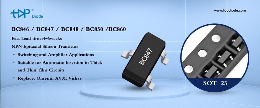
NPN:2N2222、2N3904、2N5551、BC807、BC817、BC847、MMBT2222A、BC184、BC550、MPSA42U、MMBT458、BD135、BD137、BD139
PNP:2N3906、2N2907、2N5401、2N2907A、BC560、MMBTA63、MMBT2907A、SMBTA63、FMMT734