About Schottky Barrier Rectifiers
In the most basic sense, a Schottky barrier rectifier (or simply Schottky diode) operates in the same manner as a typical semiconductor diode made from Si or Ge. However, its primary purpose is to provide rectification, i.e., allow current to flow only easily along one specific direction. In this way, they are used in typical DC circuits to enable or block current or in AC circuits as part of wave shaping.
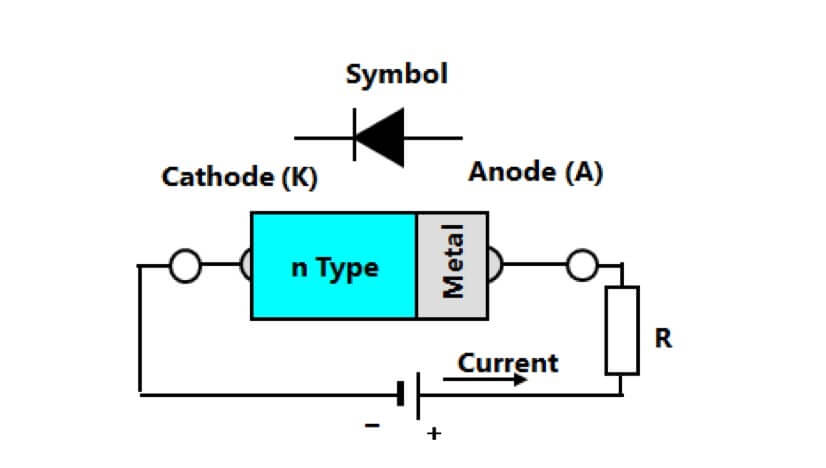
Structure
The major differences between a Schottky diode include their forward operating characteristics and, most importantly, their structure. Schottky diodes are constructed by depositing a metal electrical contact on a semiconductor; although n-type or p-type materials can be used in Schottky diodes, n-type materials are normally preferred. The reason is that p-type semiconductor Schottky diodes will have lower forward voltage and thus larger reverse bias breakdown current; using an n-type material provides the best balance between forward voltage and reverse bias current. On the other ends of the component, Ohmic contacts are placed to provide non-rectifying connections to the semiconductor.
Advantages
Compared to p-n junction diodes, Schottky barrier rectifiers have some advantages that make them more useful in switching, high-frequency rectification, and wave shaping applications. Some of the main advantages of Schottky diodes include:
1, Narrow depletion region: When forward biased, a Schottky diode will have a smaller depletion region than in a p-n diode. As a result, the junction capacitance is very low, and a Schottky diode can be switched between forward and reverse biases very quickly.
2, Lower forward voltage: A Schottky diode’s forward voltage is determined by its built-in voltage, which can be as low as 0.2 to 0.3 V. For comparison, Si p-n diodes have forward voltages of approximately 0.6 to 0.7 V, so they produce less current in forward bias.
3, Low ideality factor: Schottky diodes tend to have low ideality factor, with values as low as 1.04 being common in commercially available components.
4, Less noise: A Schottky diode will have lower nonlinear impedance in forward bias, producing less unwanted thermal noise than a typical p-n junction diode. This is one reason Schottky diodes are useful in microwave devices.
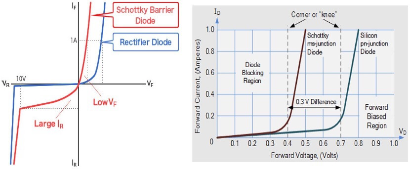
As shown below, the electrical advantages can be seen when comparing IV curves for a Si p-n diode and a Schottky diode. From here, we can see that the larger reverse bias current behavior leads to slower roll-off into the breakdown region, rather than fast avalanche behavior seen in a p-n diode.
Conclusion
Schottky Barrier Diodes offer several advantages over traditional PN-junction diodes, including low forward voltage drop, fast switching speed, low reverse recovery time, high efficiency, and high-temperature operation. These characteristics make Schottky diodes an excellent choice for a wide range of applications, particularly in high-frequency and power-sensitive circuits.
Topdiode produces high-quality Schottky Barrier Rectifiers for crossover, we have replacements for Nexperia, Diodes, SEMTECH & On-semi, please check below:
| Topdiode PN | Package | Cross to Brand | Pin to Pin Cross to P/N |
| TPDA10S65C1P | TO-220-2 | Infineon | IDH10SG60C |
| TPDA15S65C1P | TO-220-2 | Infineon | IDH16G65C6 |
| TPDB20A65C1P | TO-220-3 | On Semi | FFSP2065BDN-F085 |
| TPDD20A120C1P | TO-247-3 | Infineon | IDW20G65C5B |
| TPDD20A65C1P | TO-247-3 | Infineon | IDW20G65C5B |
| TPDD30A65C1P | TO-247-3 | Infineon | IDW32G65C5B |
| TPDD40A120C1P | TO-247-3 | On Semi | FFSH40120ADN-F155 |
| TPDG10S65C1P | TO-252 | Infineon | IDK10G65C5 |
If you want to explore more component,
please visit our website:https://www.topdiodes.com
Or send inquiry to : Luna@topdiode.com