Comparing Silicon Carbide Schottky Diodes to Silicon Diodes
Now, more than ever, Silicon Carbide (SiC) Schottky Diodes are being applied to more areas of power conversion to help significantly improve performance and energy efficiency compared to similarly rated silicon diodes. SiC Schottky Diodes are also increasingly used in power electronic circuit designs that have much higher voltages than can be accommodated by traditional silicon diodes. This widespread adoption of SiC Schottky diodes brings two other major benefits: (i) costs can be reduced, making more applications economically practical, and (ii) because of their higher efficiency modern designs can meet newly-enacted energy efficiency requirements.
Silicon Carbide Schottky Barrier Diodes (SiC SBDs) and Silicon (Si) diodes have several differences. One of the primary differences is the material used to make them. Si diodes are made from silicon, while SiC SBDs are made from silicon carbide. SiC SBDs have a lower forward voltage drop compared to Si diodes due to the absence of a depletion region, resulting in lower resistance and lower power losses. SiC SBDs also have a much shorter reverse recovery time compared to Si diodes, allowing for faster switching and lower switching losses. SiC SBDs have a higher breakdown voltage than Si diodes, making them suitable for high-voltage applications. Additionally, SiC SBDs can operate at much higher temperatures compared to Si diodes due to the high thermal conductivity of SiC and are typically smaller in size compared to Si diodes with similar ratings. These differences make SiC SBDs more suitable for high-performance applications in power electronics, automotive, aerospace and defense, renewable energy, and consumer electronics.
Compared to standard silicon bipolar diodes, SiC Schottky Diodes have negligible reverse recovery, which reduces switching losses and enables dramatic increases in system efficiency.
The Silicon Carbide Schottky Barrier Diodes differ from conventional Si Diodes in many ways which can be summarized in the table below:
| Characteristics | SiC Schottky Barrier Diode | Silicon Diode |
| Material | Silicon Carbide | Silicon |
| Forward Voltage Drop | Lower | Higher |
| Reverse Recovery Time | Shorter | Longer |
| Breakdown Voltage | Higher | Lower |
| Temperature Operation | Higher | Lower |
| Size | Smaller | Larger |
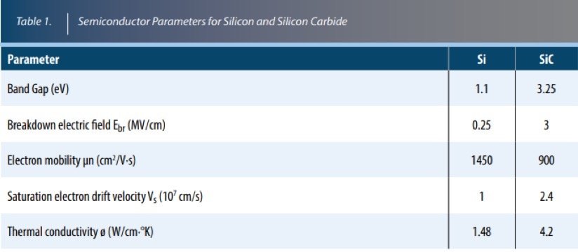
Using SiC to make Schottky Barrier Diodes (SBDs) increases the possible breakdown voltage from 200 volts to well over 1000 volts because of the high band gap of the semiconductor. Just the differences in semiconductor materials results in enhanced operational benefits for SiC Schottky diodes, which are shown in the table below:
Like all diodes, the forward voltage of a SiC Schottky Diode increases with current. The maximum current allowed is limited by the bond wires and the rate at which heat can be removed from the junction area. Since the heat produced in the junction must flow from the junction through the semiconductor material of the cathode to the mounting surface for removal, a silicon carbide semiconductor is superior at removing heat so it can run at higher maximum operating junction temperatures. An added advantage is that the SiC substrate is thinner, which makes the thermal path from the junction to the mounting surface shorter.
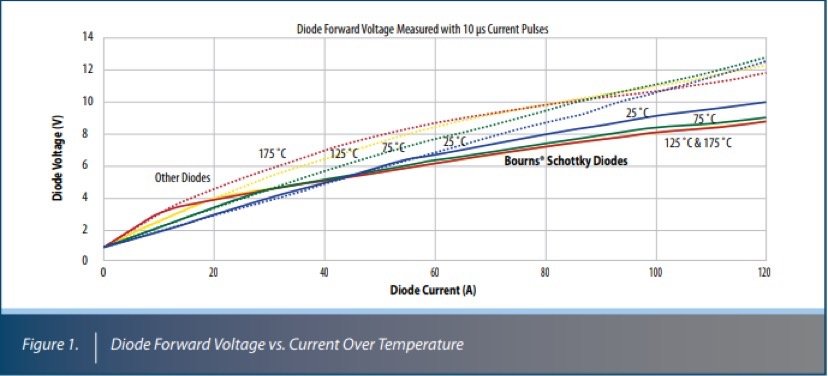
Measurements shown in Figure 1 compare Topdiode SiC Schottky Diodes and industry-standard silicon Schottky Diodes for rectangular pulse widths of 10 µs. Topdiode® SiC Schottky Diodes exhibit a negative temperature coefficient of resistance, illustrated by the decrease in forward voltage with temperature. This is beneficial when designers need to parallel two or more devices to increase the power capability to accommodate large area current sharing. The fact that the diode forward voltage and operating resistance decrease at elevated temperatures is also advantageous to help prevent thermal runaway in parallel connections
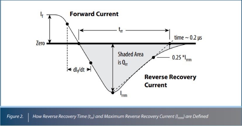
For diodes made from silicon carbide semiconductor material, the faster reverse recovery speed and reduced reverse charge recovery is a result of the lower capacitance of their internal construction. Since the diode capacitance is constant over temperature as indicated by the constant stored charge, Qrr, the reverse recovery time will be constant over temperature, which is better for stabilizing power switching applications. Figure 2 shows the definition of the reverse recovery time. When forward bias is removed, the forward current decreases and keeps on flowing past zero at a rate of dIf/dt, removing the excess charge stored in the depletion region. The reverse current is the flow of excess charge, reaching the maximum reverse recovery current, Irrm. It decreases until all the stored charge is removed. The reverse recovery time is the time required to remove the excess charge. It is measured from the beginning of the reverse current to a linearized time when the current returns to zero and the stored charge is removed
For further question or inquiries, please kindly contact Loie: sales4@topdiode.com, or visit our website: www.topdiodes.com thanks