Introduction
MOS , is the abbreviation of MOSFET. MOSFET metal-oxide semiconductor field-effect transistor, referred to as gold-oxygen half-effect transistor((Metal-Oxide-Semiconductor Field-Effect Transistor, MOSFET)
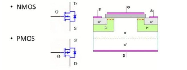
MOS transistors are divided into P-type MOS transistors and N-type MOS transistors. An integrated circuit composed of MOS transistors is called a MOS integrated circuit. A circuit composed of NMOS transistors is called an NMOS integrated circuit, a circuit composed of PMOS transistors is called a PMOS integrated circuit, and a complementary MOS circuit composed of both NMOS and PMOS transistors is called a CMOS circuit.
Field effect transistor, like transistor, also has three pins and a PN junction area inside, where P represents holes (positrons) and N represents negative electrons.
Gate S-source D-drain
Like a transistor, the direction pointed by the arrow is an N-type semiconductor
The source drain directions of PMOS and NMOS are opposite, with the drain terminal of NMOS on top and the source terminal of PMOS on top. The reason for this is to use the direction to indicate the high or low potential. The drain voltage of NMOS and the source voltage of PMOS are both higher than the gate voltage, so this annotation obtains a “visual aid”
Principle of conduction
NMOS is a grid high level (|VGS| > Vt) conduction, low level off, can be used to control the conduction between the ground.
The PMOS is a low gate (|VGS| > Vt) on-off, high level off, can be used to control the on-off between the power supply.
Due to the fact that the source terminal of NMOS is generally grounded (low potential), in order to make | VGS |>Vt, the gate terminal generally needs to be connected to a positive voltage so that the transistor can conduct;
Due to the fact that the source terminal of PMOS is generally connected to VDD (high level), in order to make | VGS |>Vt, the gate terminal generally needs to be connected to a negative voltage (low voltage with VDD), so that the transistor can conduct.
Where Vt is the turn-on voltage of the MOS transistor.
NMOS is an N-channel with a P-type substrate connected to the lowest potential, while PMOS is a P-channel with an N-type substrate connected to the highest potential. This is to form a P-N junction reverse bias between the source and drain terminals and the substrate, otherwise the current would directly conduct forward from the source and drain terminals to ground. The breakdown also refers to the reverse breakdown of this P-N junction. Because the materials of the channel and substrate are different, there is a theory of depletion inversion layer formation due to changes in gate voltage.
The channel material of NMOS is N-type, while the substrate material is P-type, so a positive voltage needs to be applied to the gate to repel holes in the P-type substrate, attract electrons to gather below the channel, and form a gate capacitor with the metal plate of the gate. The dielectric material of the capacitor is SiO2. The channel material of PMOS is P-type, while the substrate material is N-type. To attract holes in N-type material, a negative voltage should be applied to the natural gate. Just as the higher the positive gate voltage of NMOS, the stronger the conductivity of the channel, the higher the negative gate voltage of PMOS, the stronger the conductivity of the channel.
Characteristics of MOSFET
1, MOS are easily broken down. The capacitance composed of gate and P-type substrate is easily broken down by high voltage. The insulation layer between the gate and the P-type substrate is easily broken down.
2, The gate input impedance of MOS transistor is very high. This is because there is an insulation layer present, and the gate input impedance can reach hundreds of millions of ohms. So the input of MOS transistors takes almost no current, which is why many integrated circuits and chips now integrate MOS
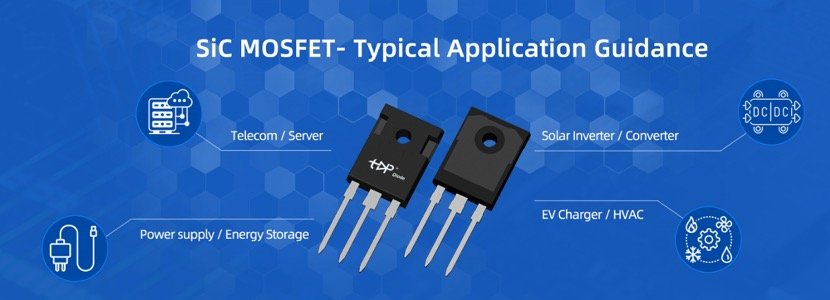
Topdiode produces PIN to PIN alternative to replace MOSFET from AOS, Onsemi, Infineon, Vishay, etc. has been supplying to GE, PNE, Jabil etc.
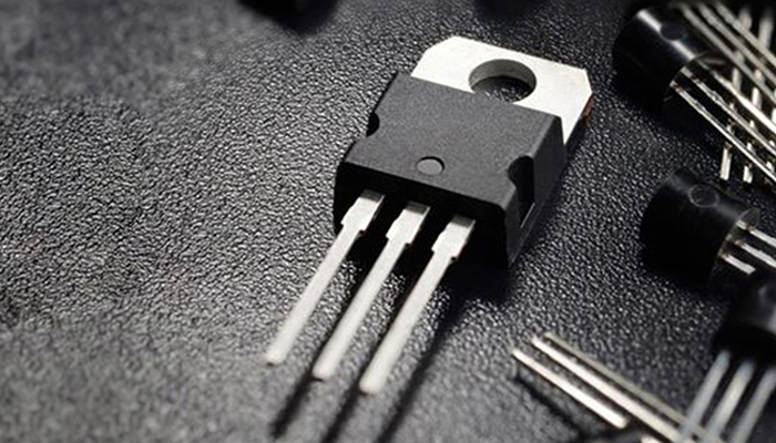
Focus in SOT-23, SOP-8, SOT-223, SOT-363, TO220, TO-252, TO-263 etc,
Cost down 30~60%, better lead ime
Engineer team to do “cross to”
Support sample in free & trial order,
1 year warranty & take responsibility after-sales.
Application
- E-HORN –Auto
- DC-DC Converters
- Power Management Functions
- Backlighting”
- Power Supply for coffee maker
- 3W electric vehicle
- motor controller”
- High current load applications.
- Two-way radio
- Routers and Switches
- Amplifier/Bluetooth speaker
| Products | Part No. | Package Type | Configuration | MOSFET Type |
Cross to Brands | Cross to P/N | Package | |
| MOSFET | TP9926 | SOP-8 | Dual | N+N | Diodes | DMN2029USD-13 | SO-8 | |
| MOSFET | TPM9435 | SOP-8 | Single | P | AOS | AO4459 | SOIC-8 | |
| MOSFET | TP4008SD | SOP-8 | Dual | N+N | AOS | AO4882 | SOIC-8 | |
| MOSFET | TP4435C | SOP-8 | Single | P | MagnaChip | MDS3652URH | SOIC-8 | |
| MOSFET | TP4435C | SOP-8 | Single | P | On Semi | FDS4435BZ | SO-8 | |
| MOSFET | TP3010 | SOP-8 | Single | N | On semi | NDS8410A | SOIC-8 | |
| MOSFET | TP4409S | SOP-8 | Single | P | Vishay | SI4401FDY-T1-GE3 | SOIC-8 | |
| MOSFET | TP4847 | SOP-8 | Dual | N+N | VS | VS5814DS | SOP-8 | |
| MOSFET | TP4409S | SOP-8 | Single | P | Infineon | IRF7240TRPBF | SO-8 | |
| MOSFET | TP4409S | SOP-8 | Single | P | Vishay | SI4401FDY-T1-GE3 | SOIC-8 |
Simply send RFQ to lily@topdiode.com for quote of MOS.
There will be experienced engineers do cross reference and choose the match series for you.