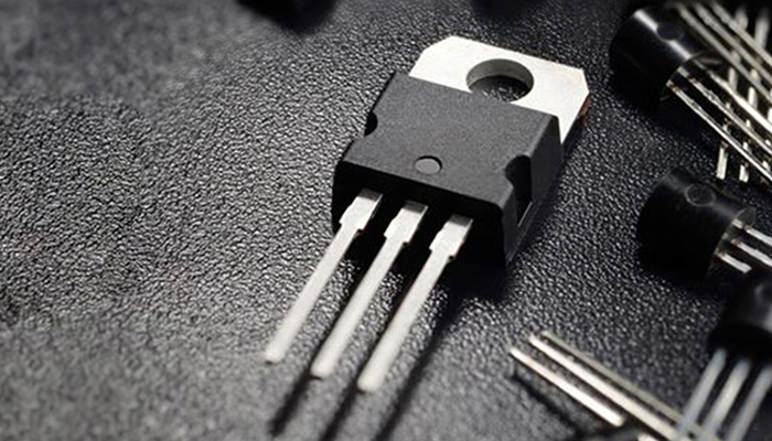
Today, let’s learn about the IGBT – the Insulated Gate Bipolar Transistor. The IGBT is a power semiconductor device used in high voltage and high current applications. They’re mainly used as switches in power electronic circuits. Did you notice that in the name of IGBT, there’s an insulated gate like in a FET and a bipolar transistor like in BJT? This is not a coincidence, and the IGBT is indeed a device fabricated trying to include the best of both transistors – particularly the MOSFET and the BJTs – making it worth looking at them from a semiconductor perspective.
Basics of IGBT
Look at the image below. Since the IGBT is a mix of the FET and the BJT, the symbol also represents this combination. A p-channel IGBT can also be represented similarly.
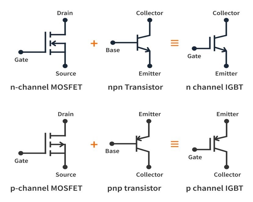
The IGBT has collector and emitter terminals similar to the BJT, where the actual current flows and an insulated gate instead of a base for controlling the device on and off.
Fabrication of the IGBT and its Structure
The n-channel IGBT’s semiconductor structure is as shown in the image below.
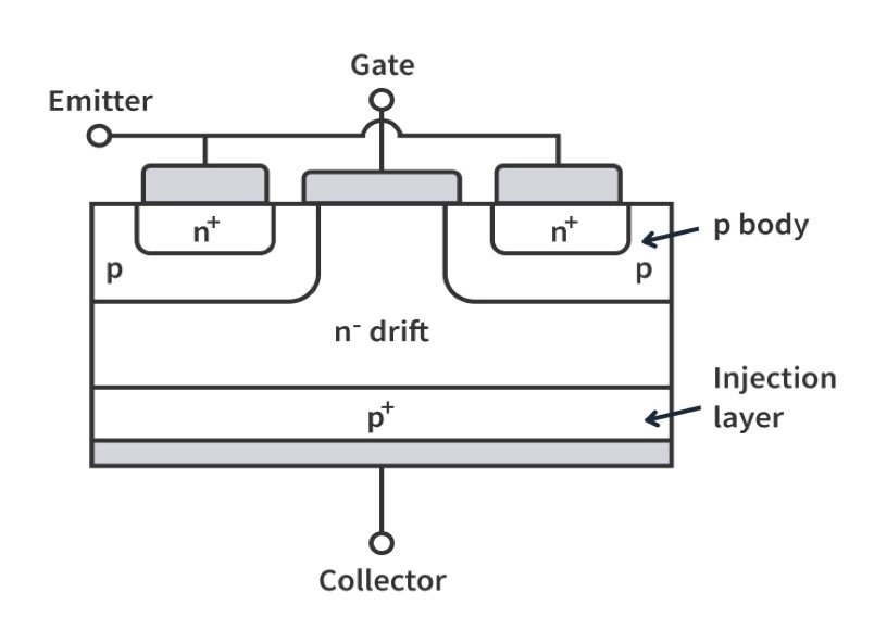
The whole structure is developed on an n-type substrate (specifically, n–type substrate – about which we’ll discuss soon). Two p-bodies are formed at the top. Two n+ wells are created inside the p-body to form the emitter terminal. The n-channel for current conduction is formed with the help of the gate at the top. A superscript of ‘+’ or ‘-’ denotes the doping concentration, with a ‘+’ indicating heavily doped and ‘-’ being lightly doped. The n– layer in the center is a very important layer. This is known as the drift layer.
When we talk about the voltage rating of a device, we are talking about the amount of reverse bias the device can handle without breaking down. The n– drift layer increases this voltage rating of the device. For the understanding of this particular EEFAQ, you have to remember that when you dope either the p side or n side or both p and n sides of the pn junction very lightly, the voltage at which the breakdown of the junction occurs under reverse bias increases significantly allowing us to increase the voltage rating of the device. Similarly, when the doping is very high on a junction, that junction breaks down easily. The base-emitter junction of a BJT breaks down easily for this very reason, as the emitter is highly doped. Hence the voltage rating of the BJT is poor.
Returning to the device structure, a p+ injection layer is fabricated at the very end of the wafer forming the collector terminal. It’s called an injection layer because it injects charge carriers (holes) into the n– drift layer to boost current flow in the overall device.
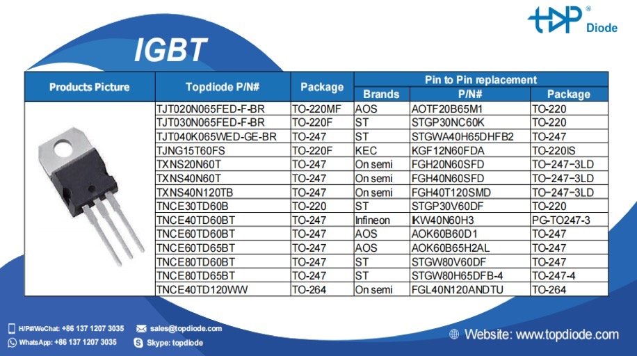
Topdiode produces high-quality IGBT for crossover, we have replacements for Nexperia, Diodes, SEMTECH & On-semi, please check below:
If you want to explore more component,
please visit our website:https://www.topdiodes.com
Or send inquiry to : Luna@topdiode.com